

pcb tutorials
Multilayer PCB Design & Layer Stackup
Feb
The Ultimate Guide to Multilayer PCB Design & Layer Stackup: Boost Your Electronics Projects
In today’s competitive electronics industry, designing a reliable, high-performance PCB requires more than just connecting components. One of the most critical factors is mastering multilayer PCB design and layer stackup, which directly impact signal integrity, EMI performance, and the overall reliability of your circuits. Whether you are building a high-speed communication device, a compact IoT gadget, or an industrial control board, understanding multilayer design is essential for success.
At NeuroCircuit, we specialize in PCB design and prototyping, and in this guide, we will share insights, practical tips, and strategies to help you achieve professional-level multilayer PCB designs.
PCB and PCBA request registration
1. What is a Multilayer PCB?
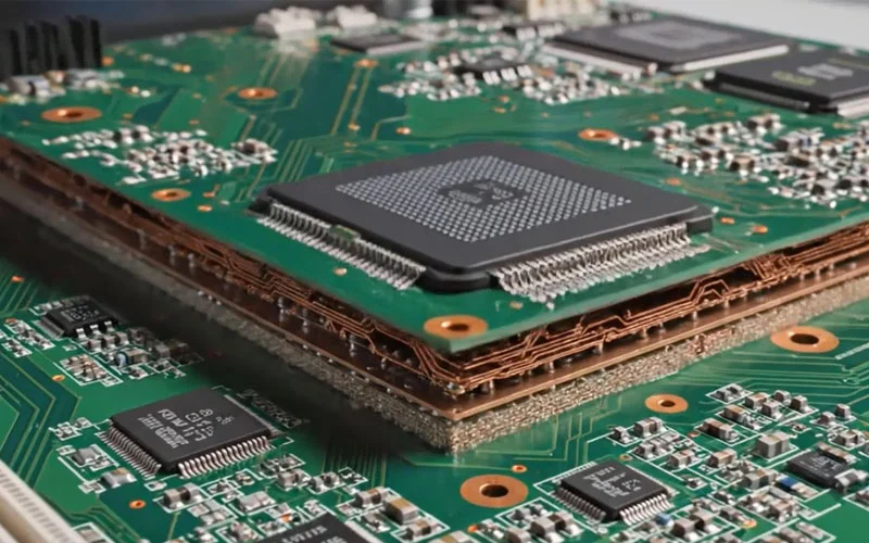
A multilayer PCB is a printed circuit board containing three or more conductive layers separated by insulating layers. Unlike single-layer or double-layer PCBs, multilayer boards allow higher circuit density and more complex designs without increasing board size.
Key benefits of multilayer PCBs include:
-
Compact designs for modern electronics
-
Improved signal integrity and reduced crosstalk
-
Enhanced power distribution across layers
-
Efficient thermal management
These advantages make multilayer PCBs the go-to solution for industries like aerospace, telecommunications, robotics, and automotive electronics.
2. Why Layer Stackup is Crucial
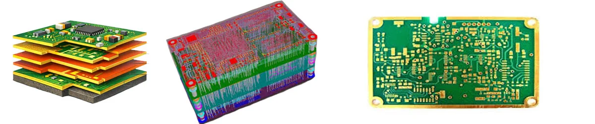
The layer stackup refers to the arrangement of conductive (signal, power, ground) and insulating layers in a multilayer PCB. It is one of the most overlooked yet crucial aspects of PCB design. A proper stackup ensures:
-
Signal integrity: Reduces signal reflection, crosstalk, and timing issues
-
Power stability: Dedicated power and ground planes minimize voltage drop and noise
-
Electromagnetic compatibility (EMC): Minimizes EMI and meets regulatory standards
-
Thermal performance: Ensures effective heat dissipation for high-power components
A poorly planned stackup can result in failed prototypes, costly rework, and unreliable products.
3. Common Multilayer PCB Configurations
Depending on complexity, different multilayer configurations are used:
4-Layer PCB Stackup:
-
Top Layer: Signal
-
Inner Layer 1: Ground Plane
-
Inner Layer 2: Power Plane
-
Bottom Layer: Signal
Ideal for high-speed digital circuits, offering a balance between performance and cost.
6-Layer PCB Stackup :
-
Top Layer: Signal
-
Inner Layer 1: Ground Plane
-
Inner Layer 2: Signal
-
Inner Layer 3: Power Plane
-
Inner Layer 4: Signal
-
Bottom Layer: Signal
Best for complex boards requiring multiple power rails and higher routing density.
8-Layer PCB Stackup and Beyond :
Used in advanced computing, RF circuits, and high-frequency applications, providing multiple power and ground planes for optimal signal integrity and EMI control.
4. How to Choose the Right Stackup
Selecting a stackup depends on project requirements:
-
Signal type: High-speed or RF signals need dedicated ground and power planes
-
Frequency: High-frequency circuits require controlled impedance
-
Board size: Multilayer PCBs save space in compact devices
-
Budget: Each additional layer increases manufacturing cost
Pro tip: Always simulate your stackup in tools like Altium Designer, KiCad, or Eagle before production to ensure performance and manufacturability.
5. Key Design Considerations for Multilayer PCBs
Material Selection
The dielectric material affects impedance, signal loss, and thermal performance. Common materials:
-
FR4: Standard, cost-effective
-
Rogers, Polyimide: For high-frequency or high-speed designs
Impedance Control
Maintaining controlled impedance ensures signal integrity and avoids reflection and crosstalk.
Via Management
Vias connect layers but introduce inductance and capacitance. Consider:
-
Blind/buried vias for high-density boards
-
Minimizing via count on critical traces
Thermal Management
Power planes help dissipate heat. High-power components may require thermal vias or heat sinks.
Grounding and Power Distribution
Dedicated ground planes reduce noise. Multiple power planes support different voltage levels and improve stability.
PCB and PCBA request registration
6. Multilayer PCB in Modern Electronics
Today’s devices are smaller, faster, and more complex:
-
Smartphones and laptops often use 6-8 layer boards
-
IoT devices require compact, high-density layouts
-
Industrial controllers and robotics rely on signal integrity and EMI control
Without proper stackup design, your board may fail EMI tests, experience signal degradation, or have thermal issues, leading to costly production delays.
7. How NeuroCircuit Can Help Your PCB Projects
At NeuroCircuit, we provide end-to-end multilayer PCB solutions:
-
Professional Layer Stackup Planning: Reduce EMI, improve signal integrity, and optimize thermal performance
-
PCB Design Services: From schematic capture to layout and DRC checks
-
Prototyping & Manufacturing: High-quality boards with reliable performance
-
Custom Solutions: For IoT, robotics, industrial electronics, and high-speed circuits
Why choose us?
-
Experienced engineers with real-world PCB design expertise
-
Optimization for both performance and manufacturability
-
Support from design to production with quality assurance
Whether you’re building a robotics controller, IoT device, or RF board, our team ensures your PCB performs flawlessly and meets industry standards.
8. Practical Tips for Multilayer PCB Designers
-
Simulate Your Design Early: Identify signal integrity issues before manufacturing
-
Use Professional Tools: Software like Altium Designer or KiCad helps simulate impedance, check DRC, and manage complex stackups
-
Optimize Trace Width and Spacing: Critical for high-frequency and high-power circuits
-
Separate Analog and Digital Traces: Reduces noise and improves reliability
-
Document Your Stackup: Keep a clear record for fabrication and assembly
9. Future of PCB Design and Layer Stackup
With electronics moving toward smaller, faster, and multi-functional devices, multilayer PCBs are no longer optional. Advanced tools, AI-assisted routing, and simulation software are helping engineers reduce errors, save time, and improve reliability.
Investing in professional multilayer design today ensures your electronics are ready for tomorrow’s challenges.
10. Conclusion: Start Optimizing Your Multilayer PCB Today
Mastering multilayer PCB design and layer stackup is crucial for building reliable, high-performance electronics. The right stackup ensures:
-
Excellent signal integrity
-
Stable power distribution
-
Effective thermal management
-
Reduced EMI and noise
With guidance from NeuroCircuit, your PCB can reach its full potential, from concept to production, while staying cost-effective.
Contact us today and take the first step toward professional multilayer PCB design that performs flawlessly in real-world applications.