
pcb tutorials
10 Common PCB Design Mistakes That Can Ruin Your Project

Feb
After completing a PCB design, many designers discover that the real challenges are just beginning. A board that looks perfect in the schematic and layout phase may behave unpredictably once powered on. Random resets, noise issues, EMI problems, and unstable performance often appear due to weaknesses in grounding, PDN structure, or decoupling strategy.
At the same time, unexpected technical issues can quickly translate into higher costs and serious project delays. Board revisions, rework, and repeated testing cycles push deadlines further out and increase pressure from clients or management.
Even more frustrating is when a board that worked flawlessly in the lab begins to fail in real-world conditions. Heat, actual load variations, industrial noise, or the realities of mass production can expose weaknesses that were not visible during prototyping.
These technical failures don’t just affect the hardware—they impact professional credibility. When a product underperforms or fails in the field, customer trust declines, and the engineer’s reputation can suffer.
Finally, poor testability can turn every issue into a time-consuming investigation. Without proper test points or a clear debugging strategy, troubleshooting becomes slow, expensive, and exhausting.
In short, the biggest challenge after design is not drawing the board—it’s ensuring that it performs reliably, can be manufactured smoothly, and remains stable in real operating conditions.
You can listen to this article as an audio
The good news is that most of these post-design problems are preventable. By simply following the 10 essential design principles outlined in the next section, designers can dramatically reduce instability, costly revisions, production risks, and debugging time. These principles are not complicated or theoretical—they are practical rules that, when applied consistently, can significantly improve reliability, manufacturability, and overall project success.
And now, the 10 essential principles you must follow during PCB design:
1 – Poor Ground Design and Improper Return Current Path
One of the most serious yet often overlooked mistakes in PCB design is misunderstanding the concept of ground. Many designers—especially in small projects or early prototypes—assume that simply connecting all ground points to a net labeled GND is sufficient. In reality, ground is an active return path for current, and its behavior is highly dependent on signal frequency and board topology.
Every signal that travels along a track must return to its source through a return path. In simple DC circuits, this path may not seem critical. However, in digital systems with fast edges, even if the operating frequency is relatively low, the signal contains high-frequency components that significantly affect circuit behavior.
Return current naturally follows the path of least impedance, which in multilayer PCBs is typically directly beneath the signal track on a continuous ground plane. If this plane is fragmented, contains gaps, or if a signal crosses a split plane, the return path is forced to detour. This detour increases the loop area, raises path inductance, and ultimately leads to higher EMI and noise.
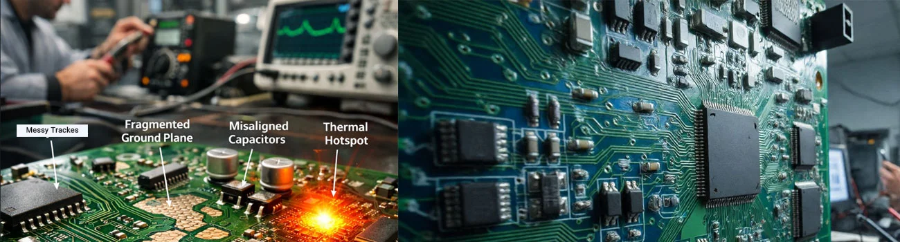
A common scenario in industrial projects is the random reset of a microcontroller when power loads switch on or off. In many cases, the root cause is poor ground design and shared return paths between power and signal currents.
Practical solutions include using a solid, uninterrupted ground plane, preventing high-speed signals from crossing plane splits, and carefully analyzing return current paths before manufacturing the board.
Ignoring this issue can lead to costly board revisions, project delays, and even the loss of customer trust.
2 – Incorrect Placement of Decoupling (Bypass) Capacitors
Another common and costly mistake in PCB design is the improper placement of decoupling (bypass) capacitors. Many designers assume that simply placing a 100nF capacitor on each IC is sufficient. However, the location of the capacitor is just as important as its value.
The purpose of a decoupling capacitor is to quickly supply the instantaneous current required by the IC during internal switching. When a microcontroller or FPGA changes its logic state, short but high-current spikes occur. If this current cannot be supplied by a nearby capacitor, it must travel through longer paths from the power source, causing voltage dips and introducing noise on the power line.
Placing a capacitor several centimeters away from the VCC pin practically renders it ineffective, because the track inductance between the capacitor and the IC pin slows its response.
In high-speed boards or high-power processors, it is essential to use multiple capacitors of different values—such as 100nF, 1µF, and 10µF—in parallel and as close as possible to the power pins.
In many unstable boards or those that experience issues at power-up, simply reviewing and correcting the placement of bypass capacitors has solved the problem.
Proper power supply design is a fundamental pillar of system stability and should never be considered a minor detail.
3 – Selecting Inadequate track Width for Current Carrying
One mistake that is often less noticeable in prototypes but becomes problematic in mass production is selecting an improper track width for current-carrying paths.
Every PCB track has a certain resistance, which depends on its length, width, copper thickness, and operating temperature. If the current flowing through the track exceeds its capacity, the track heats up. This temperature rise can lead to voltage drops, changes in circuit behavior, and even track burnout.
This issue is especially critical in power boards, motor drivers, switching power supplies, and charging circuits. Sometimes, designers make decisions based solely on the visual appearance of the track, assuming it is wide enough without performing precise calculations.
Online tools are available to calculate the appropriate track width according to IPC standards, and these should always be used during the design phase. Designers must also consider temperature rise under real environmental conditions.
In industrial projects, there have been cases where power tracks gradually changed color and their resistance increased after a few months of operation at elevated temperatures, ultimately leading to complete device failure. Professional PCB design means considering worst-case operating conditions, not just ideal lab scenarios.
4 – Poor High-Speed Routing and Lack of Impedance Control
As signal speeds increase, a PCB is no longer just a simple copper board—it becomes a signal transmission medium with frequency-dependent behavior. Many designers assume that if the circuit operates at a low frequency, high-speed design rules are unnecessary. However, what really matters is the signal edge rate, not just the operating frequency.
For example, a 10 MHz digital signal with very fast edges can contain frequency components in the hundreds of MHz range. If tracks are not treated as transmission lines, phenomena such as reflection, ringing, and overshoot can occur.
A common mistake is failing to control the impedance of sensitive tracks like USB, HDMI, Ethernet, or high-speed SPI lines. If the track impedance does not match the source and load, part of the signal is reflected, reducing signal quality.
Another issue is length mismatch in differential pairs or parallel buses. Even a few millimeters of difference can cause skew and data errors.
Practical solutions include:
• Using an appropriate reference layer
• Calculating track width based on target impedance
• Maintaining proper spacing between differential pairs
• Avoiding unnecessary vias
Ignoring these principles may work in prototypes but will cause significant problems in mass production or in electrically noisy industrial environments.
5 – Poor Component Placement
Many designers focus primarily on routing, while the quality of a PCB depends more than anything on proper component placement. In fact, if components are placed correctly, routing becomes simpler, shorter, and cleaner.
A common mistake is arranging components purely for visual appeal or overly compacting them. Placement, however, should consider signal flow, circuit operation sequence, and noise-sensitive areas.
For example:
• Analog paths should be short and kept away from noise sources.
• Power circuits should be concentrated in a dedicated area.
• Bypass capacitors must be placed as close as possible to IC power pins.
• Microcontroller crystals should be located near their respective pins.
Poor placement can cause even the best schematic design to behave unreliably. In industrial projects, sometimes simply rearranging components—without changing the schematic at all—can dramatically improve system performance.
A golden rule in PCB design is: good routing cannot compensate for poor placement.
6 – Ignoring Thermal Management
Heat is one of the main enemies of electronic components. However, many designers focus solely on electrical performance and overlook the thermal behavior of the board.
Components such as regulators, MOSFETs, drivers, and processors generate significant heat. If this heat is not properly dissipated, junction temperatures rise, drastically reducing component lifetime.
Common mistakes in this area include:
• Not using thermal vias under power component pads
• Underestimating copper area for heat sinking
• Overcrowding power components
• Ignoring airflow inside the enclosure
In some projects, a device may appear perfectly stable on the bench, but once placed in its final enclosure and operating at high ambient temperatures, it may fail.
Professional thermal design involves:
• Estimating power dissipation
• Predicting temperature rise
• Using large copper areas for heat spreading
• Considering real environmental conditions
Neglecting thermal management can lead to gradual, hard-to-detect failures that damage product reliability and reputation.
7 – Excessive Use of Vias and Unnecessary Layer Changes
Vias are powerful tools in PCB design, but excessive use can cause serious problems. Every via has its own inductance and resistance, which can degrade performance in high-speed or high-current paths.
In multilayer designs, some designers move signals between layers multiple times without a clear plan. This not only increases manufacturing complexity but also disrupts the return current path.
In differential pairs, a mismatch in the number of vias between the two tracks can cause asymmetry, reducing signal quality.
Additionally, excessive vias:
• Increase manufacturing costs
• Raise the likelihood of production errors
• Make testing and debugging more difficult
Vias should be used judiciously, with a clear understanding of their impact on signal integrity and overall cost.
8 – Poor Power Distribution Network (PDN) Design
Many designers assume that selecting the correct voltage regulator solves power supply issues. However, a well-designed Power Distribution Network (PDN) is one of the most critical parts of a PCB.
Every IC consumes fast, short-duration transient currents during switching. If the power path has high impedance, instantaneous voltage drops occur. These drops can lead to unpredictable behavior, system resets, or data errors.
Common mistakes include:
• Using narrow tracks for high-current ICs
• Not using power planes in multilayer boards
• Sharing analog and digital power paths without proper separation
• Failing to analyze peak current demands
In FPGA-based or high-speed processor systems, voltage drops of just a few tens of millivolts can disrupt performance. In industrial projects, devices that were stable in initial testing have experienced random resets in noisy environments or under changing temperatures.
Professional PDN design includes:
• Using low-impedance power planes
• Distributing decoupling capacitors across multiple frequency ranges
• Keeping power paths as short as possible
• Estimating the network’s approximate impedance
A professional designer always asks:
“If all ICs switch simultaneously, will my power supply remain stable?”
9 – Ignoring DFM (Design for Manufacturing) Principles
One of the biggest mistakes that beginners often make is designing a PCB without considering manufacturability. A board that looks perfect in software may encounter serious issues during mass production.
DFM means designing a board in a way that:
• Simplifies manufacturing
• Reduces production errors
• Lowers cost
• Increases yield
Common DFM mistakes include:
• Track spacing below the manufacturer’s capability
• Excessive use of small vias without necessity
• Choosing track widths that are unstable in mass production
• Designing pads that complicate automated assembly
Sometimes designers follow only the software’s minimum rules rather than the manufacturer’s limits. The result? The board may work in prototyping but experience high failure rates in mass production. In commercial projects, DFM directly affects profitability—each percent drop in yield can significantly increase production costs. Professional designers always verify the manufacturer’s rules before sending Gerber files.
10 – Poor Testability and Lack of Debug Planning
This mistake may be the most costly of all.
Many designers create a board without considering testing and debugging. When an issue arises, they discover that accessing critical signals is nearly impossible.
Common mistakes in this area include:
• Lack of test points for key signals
• Inadequate access to UART or debug ports
• Overcrowding components, making oscilloscope probing difficult
• Removing temporary connectors to save cost
In industrial projects, debugging can take several times longer than design. If a board is difficult to test, troubleshooting can take weeks.
A professional designer always asks:
• If this board fails, how will I debug it?
• Can I measure the current of each section separately?
• Are critical signals easily observable?
Adding a few small test points during the design phase can save hours or even days during debugging.
To download the full version of this practical tutorial, simply enter your email and download it now.
If you want to learn PCB design in a practical and proper way, we offer a training course that will help you master standard and professional design techniques.
Click here to access the course or scan the QR code below.