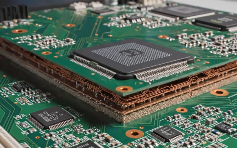
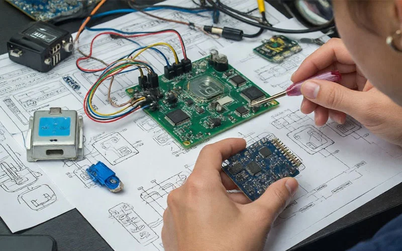
After completing a PCB design, many designers discover that the real challenges are just beginning. A board that looks perfect in the schematic and layout phase may behave unpredictably once powered on. Random resets, noise issues, EMI problems, and unstable performance often appear due to weaknesses in grounding, PDN structure, or decoupling strategy. At the […]
Category Archives: pcb tutorials
PCB design and development training
The Ultimate Guide to Multilayer PCB Design & Layer Stackup: Boost Your Electronics Projects In today’s competitive electronics industry, designing a reliable, high-performance PCB requires more than just connecting components. One of the most critical factors is mastering multilayer PCB design and layer stackup, which directly impact signal integrity, EMI performance, and the overall reliability […]


